

2D materials and van der Waals (vdW) heterostructures are promising candidates to build efficient THz spintronic emitters. Here, we demonstrate the drastic modification of THz spintronic emission by inserting a single layer of MoSe2 in the PtSe2/graphene vdW heterostructure. Ab initio calculations indeed show the emergence of Rashba states due to the electronic hybridization between MoSe2 and PtSe2 giving rise to strong spin-to-charge conversion and THz emission.

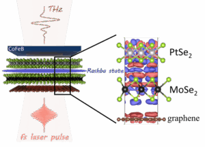
Illustration of the hybridization between MoSe2 and PtSe2 monolayers generating Rashba states at the interface governing THz spintronic emission.
Spintronics is being more and more integrated into THz technologies enabling more energy efficient and tunable THz emission. The underlying mechanism of spintronic THz emission is spin-to-charge conversion. In this respect, 2D materials present several key advantages like Rashba or topological spin textures, large spin-orbit coupling, various crystal symmetries and their electronic properties can be easily manipulated with strain, light or electric fields. In this work, we show that THz spintronic emission can be efficiently manipulated at the atomic scale in vdW heterostructures. For this, we insert a single layer of MoSe2 in the PtSe2/graphene vdW heterostructure which modifies both the sign and intensity of THz emission owing to the formation of Rashba states at the hybridized interface between MoSe2 and PtSe2.
We use molecular beam epitaxy (MBE) in the van der Waals regime to grow PtSe2/graphene and PtSe2/MoSe2/graphene epitaxial vdW heterostructures on SiC substrates. Both stacks are covered with a thin ferromagnetic CoFeB layer serving as the spin source and 4 nm of Al to protect the films against oxidation, both evaporated by sputtering. THz time-domain spectroscopy is performed by exciting the stacks with 80 fs laser pulses at 800 nm with linear polarization. THz pulses are detected with a 250 µm-thick ZnTe crystal. We first observe a weak positive THz emission from PtSe2/graphene. Using ab initio calculations, we could attribute this signal to the Rashba effect at the PtSe2/graphene interface owing to interface charge transfer and the formation of an electric dipole. Surprisingly, by inserting a single layer of MoSe2 between PtSe2 and graphene, we could detect a 3.5 times larger THz emission with opposite sign. To explain this result, we perform spin-ARPES measurements with synchrotron radiation and ab initio calculations to unveil the strong electronic hybridization between MoSe2 and PtSe2 owing to their epitaxial relationship. We thus demonstrate that, despite the vdW gap, electronic hybridization takes place at the interface between 2D semiconductors leading to the formation of Rashba states as illustrated in the figure. These Rashba states are responsible for spin-to-charge conversion and the enhanced THz emission.
Our results open perspectives for the manipulation of THz spintronic emission at the atomic scale using 2D materials vdW heterostructures.
Team: 2D Spintronics, Theory and Materials growth (plateforme Cluster 2D)
Collaboration: Laboratoire de Physique de l’ENS (Paris), Laboratoire Albert Fert (Palaiseau), IRIG-MEM (Grenoble), ELETTRA (Trieste, Italie), CEA LETI (Grenoble), C2N (Palaiseau)
Funding: ESR/EQUIPEX+ ANR-21-ESRE-0025 2D-MAG projects, PEPR SPIN ANR-22-EXSP-0003 TOAST, PEPR SPIN ANR-22-EXSP-0009 SPINTHEORY
Further reading: Monolayer control of spin-charge conversion in van der Waals heterostructures, K. Abdukayumov, O. Paull, M. Mičica, F. Ibrahim, L. Vojáček, A. Wright, S. Massabeau, F. Mazzola, V. Polewczyk, C. Jego, R. Sharma, C. Vergnaud, A. Marty, I. Gomes de Moraes, A. Ouerghi, H. Okuno, A. Jana, I. Kar, J. Fujii, I. Vobornik, L. Melo Costa, O. Renault, J. Li, F. Bonell, M. Chshiev, M. Bibes, J.-M. George, H. Jaffrès, S. Dhillon and M. Jamet, Phys. Rev. Lett. 135, 016702 (2025).
Contact: Matthieu Jamet, Mairbek Chshiev