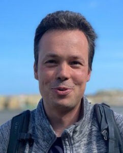
 On Monday September 22th 2025, we have the pleasure to welcome in SPINTEC Fabrice Oehler from C2N-CNRS Palaiseau. He will give us a seminar at 14:30 entitled :
CVD growth and properties of bi-dimensional chalcogenides
Place : IRIG/SPINTEC, auditorium 445 CEA Building 10.05 (presential access to the conference room at CEA in Grenoble requires an entry authorization. Request it before September 12th at admin.spintec@cea.fr)
video conference : https://univ-grenoble-alpes-fr.zoom.us/j/98769867024?pwd=dXNnT3RMeThjYStybGVQSUN0TVdJdz09
Meeting ID: 987 6986 7024
Passcode: 025918
Abstract : Bi-dimensional (2D) materials are sometimes presented as special class of compounds with little in common with their three dimensional (3D) counterparts. Yet, there is a discrete but near continuous evolution as one reduces the thickness, layer by layer, from the bulk form (3D) to the final single mono-layer (2D). In this talk, I will start by examples of such evolution and how the related electronic band structure is affected by the overall thickness reduction.
One of the current limits of 2D materials is our capacity to manufacture them over large surfaces, with a low-enough defect density while maintaining the critical thickness control. We will focus here on Chemical Vapor Deposition (CVD) and the chalcogenides family (WSe2, WS2, WTe2, etc…), highlighting the possibilities of this technique for the direct growth of single, bi-layer and ternary alloys. We will see that the growth facilities must be associated to a quite an array of characterization tools (Raman, PL, TEM, SHG) to correctly identify and assess the quality of the grown material, whether it is aimed at fundamental research or at device fabrication.
References :
- Di Berardino et al. Physical Review B, 2025, 111,125403 10.1103/physrevb.111.125403
- Mahmoudi et al. Physical Review B, 2024, 110, 165418 10.1103/physrevb.110.165418
- Mahmoudi et al. Physical Review B, 2023, 108, 045417 10.1103/physrevb.108.045417
Biography : Fabrice Oehler is a researcher at CNRS – Centre for Nanoscience and Nanotechnology (Palaiseau, France), working in the Materials Dpt. My activities have always been centered on crystal growth, since my PhD on Si nanowires by CVD (CEA Grenoble, FR), post-doc on GaN thin film MOCVD (University of Cambridge, UK) and earlier works on III-V nanostructures by MBE (CNRS LPN/C2N, FR). Since 2019, I have joined the 2D materials team at C2N to install and develop the CVD growth of 2D materials based on transition metal dichaldogenides.
Bibliography : Google scholar Orcid


