Overview
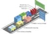
The 2D spintronics team is developing the large area growth of 2D materials by molecular beam epitaxy (MBE). Our aim is to study fundamental magnetic and spin transport properties of 2D transition metal dichalcogenides down to the monolayer limit or in van der Waals heterostructures. The main research topics are two-dimensional magnetism, spin-charge interconversion phenomena, magnetic doping and the integration of 2D materials in devices. The strength of the team relies on its long experience in the physics of 2D materials and on a unique (in France and Europe) MBE platform to grow 2D materials and vdW heterostructures on large area.
Research topics
2D magnets
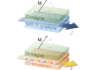
MBE growth of 2D ferromagnets and fundamental study of two-dimensional magnetism: effects of low-dimensionality (down to one monolayer) and low symmetries, manipulation by electric field and strain, proximity effects, topological effects, new spin textures (ex. skyrmions).
Spin-charge interconversion
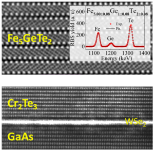
Fundamental study of spin-charge interconversion phenomena in 2D materials and van der Waals heterostructures using spin pumping, THz spintronic emission and spin-orbit torques.
Magnetic doping
Development of magnetic and electrical doping to synthesize 2D diluted magnetic semiconductors (DMS) or to reach electronic bands with specific spin texture.
2D material integration
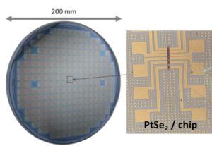
Integration of 2D materials in RF transistors, RF switches and memristors. Optimization of carrier mobility and electrical switching processes.
The team


Former members
Post-docs
- Minh-Tuan DAU (2016-2018)
- Emilio VELEZ-FORT (2019-2020)
- Mario RIBEIRO (2020-2021)
- Jules COURTIN (2022)
- Vincent POLEWCZYK (2023)
PhD
- Fabien RORTAIS (2013-2016)
- Thomas GUILLET (2017-2020)
- Quentin GUILLET (2020-2023)
- Khasan ABDUKAYUMOV (2020-2023)
Internships
- Takeo KOIKE (Sept.-Nov. 2017)
- Mohamed Husein (Mar.-Aug. 2022)
Projects
- ANR COME ON (2023-2025)
- ANR ELMAX (2021-2023)
- ANR-DFG MagSta2D (2023-2025)
- ANR NEXT (2024-2026)
- PEPR Microélectronique ADICT (2023-2027)
- Equipex 2D MAG (2021-2028)
- H2020 Graphene Flagship (-2023)
- H2020 EIC Pathfinder PLASNANO (2023-2025)
- H2020 FET-OPEN NANOPOLY (2018-2022)
- FLAG ERA MNEMOSYN
- ANR MAGICVALLEY (2018-2021)
- ANR GEMO (2008-2010)
- RTRA IMAGE (2009-2011)
- ANR SiGeSPIN (2014-2017)
- ANR MoS2ValleyControl (2015-2017)
- ANR TOP-RISE (2017-2020)
- Projet Phare CEA DRF-DRT 2D Factory (2015-2019)
- Projet CARNOT H2D3D (2017-2019)
Partners
- IRIG/PHELIQS, MEM, SYMMES, Grenoble, France
- CEA LETI, Grenoble, France
- Laboratoire Albert Fert, Palaiseau, France
- Institut NEEL, Grenoble, France
- Laboratoire Charles Coulomb, Montpellier, France
- Laboratoire de Physique de l’ENS, Paris, France
- LPCNO, INSA, Toulouse, France
- IJL, Nancy, France
- LPS, Orsay, France
- LNCMI, Toulouse, France
- Politecnico di Milano, Milan, Italy
- Forschungszentrum Jülich, Germany
- ICN2, Barcelone, Espagne
Recent news
- Review – Two-dimensional materials prospects for non-volatile spintronic memories (August 17th, 2022)
H. Yang✉, S. O. Valenzuela✉, M. Chshiev, S. Couet, B. Dieny, B. Dlubak, A. Fert, K. Garello, M. Jamet, D.-E. Jeong, K. Lee, T. Lee, M.-B. Martin, G. S. Kar, P. Sénéor, H.-J. Shin, S. ... - PEPR Electronics – Priority Programs and Equipment for Research (July 29th, 2022)
SPINTEC involved in the PEPR electronics recently funded by the French government in the framework of the national France 2030 strategy On July 12, 2022, the President of the Republic presented in Crolles the ... - PEPR SPIN – Priority Programs and Equipment for Exploratory Research (July 29th, 2022)

France is investing more than 38M€ in Spintronics thanks to the PEPR-SPIN exploratory program! SPIN is among the 13 new exploratory programs winners of the second wave of calls for projects Priority Programs and ... - MNEMOSYN – FLAG-ERA Graphene Basic Research project (July 04th, 2022)
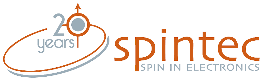
MNEMOSYN stands for « 2D MagNEtic meMOries: Scalable growth and hYbrid electrical operatioN ». It is 36-months-long FLAG-ERA Graphene Basic Research project. MNEMOSYN will develop and optimize techniques to grow large-scale 2D magnets, co-integrated with strong ... - Large-scale epitaxy of the van der Waals room-temperature ferromagnet Fe5GeTe2 (April 21st, 2022)
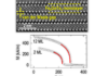
Van der Waals (vdW) layered magnets are promising materials to develop ultracompact and multifunctional spintronics devices. However, most of them are magnetic only at low temperature and are almost exclusively studied in the form of ...
Publications
For the full list of publications See the personal webpage of Matthieu JAMET, Alain MARTY and Céline VERGNAUD.