
 B. Dieny, R.C. Sousa, J.P. Nozières, O. Redon, I.L. Prejbeanu, Magnetic Random Access Memories (Ch.28), in Nanoelectronic and Information Technology, R. Waser Ed., Wiley-VCH (2011). ISBN: 978-3-527-40927-3.
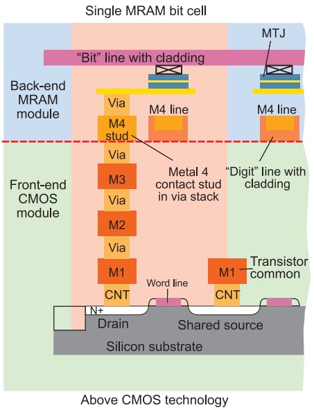
Spinelectronics is a rapidly expanding area of research and development which merges magnetism and electronics (See Chapter 4 for insights on the related basics). Since the discovery of Giant Magnetoresistance in 1988, several breakthroughs have further boosted this field (spin-valves 1990, tunnel magnetoresistance 1995, spin transfer 1996, voltage controlled magnetic properties 2004). The phenomenon of spin-transfer is particularly attractive both from fundamental and applied view points. It provides a new way to manipulate the magnetization of magnetic nanostructures by a spin-polarized current. Spinelectronics has found applications in hard disk drives (1998) and more recently in non-volatile memories (MRAM = Magnetic Random Access Memory). In MRAM, each cell consists of a magnetic tunnel junction (MTJ) connected in series with a CMOS selection device, most often a MOSFET. The information is encoded via the orientation of the magnetization of the MTJ storage layer relatively to that of the MTJ reference layer. The first generations of MRAM were based on magnetic field writing. However, these memories have a large power consumption and face downsize scalability issues. The spin-transfer phenomenon provides a new write scheme in MRAM yielding a much better scalability of these devices towards and below the 22 nm node. Thermal assistance provided by the Joule heating around the tunnel barrier can also be used to improve the MRAM performances.
Another type of memories called RaceTrack Memories were also proposed in 2004. These memories are shift registers. The information is encoded as magnetic domains along magnetic nanowires. These memories take advantage of another property associated with spin transfer effect: the possibility to move the entire pattern of domain walls coherently along the length of the nanowire thanks to a current flowing through the wire. Additional write and read elements in contact with the nanowire allow generating the domain pattern and reading it out. This chapter is devoted to these various MRAM technologies based on magnetic tunnel junctions and to racetrack memories.