Spin-charge conversion phenomena harnessing the spin orbit coupling are promising for the future of spintronics, allowing in one way (charge–to-spin) the generation of torque on magnetic elements and in the other way (spin-to-charge) the detection of spin current for spin logic or neuromorphic operations. We report a highly tunable and record spin-to-charge conversion in a simple system, consisting of an aluminum layer deposited on a SrTiO3 substrate, and map its dependence on the SrTiO3 band structure.
While spintronics has traditionally relied on ferromagnetic metals as spin generators and detectors, spin-orbitronics exploits the efficient spin-charge interconversion enabled by spin-orbit coupling in non-magnetic systems. This is providing new opportunities for devices, such as the MESO transistor proposed recently by Intel, which relies on writing of magnetic information through magnetoelectric coupling, and reading it by spin-charge conversion.
For the latter, oxide 2DEGs are promising as their spin-charge conversion efficiency is large (see our earlier work with LaAlO3/SrTiO3 2DEGs). In a new paper published in Nature Materials, we demonstrate a very large spin to-charge conversion effect in an high carrier-density SrTiO3 2DEG generated by the sputter-deposition of Al at room temperature, and map the dependence of this effect to the band structure (as measured by ARPES). We show that the conversion process is amplified by enhanced Rashba-like splitting due to orbital mixing, and in the vicinity of avoided band crossings with topologically non-trivial order.
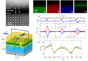
Figure 1. High resolution scanning transmission image of the NiFe/Al/SrTiO3 interface with elemental EDX spectra (top). Schematic of the dynamical spin injection and spin charge conversion (left). At ferromagnetic resonance, a spin current is injected into the 2D electron gas and converted into a transverse charge current by the inverse Edelstein effect. (b) The three panels correspond to experiments made at different back gate voltages. (d) Evolution of the conversion yield, expressed as the inverse Edelstein length, as a function of the back gate voltage applied to the SrTiO3 substrate.
Our results also alleviate the need of high quality crystalline growth of the LAO oxide layer that is usually required for the formation of the 2DEG at the STO surface. Moreover, due to the multi-orbital nature of STO, a gate voltage allows tuning the conversion, both in sign and in amplitude. Respect to our previous results a zero gate voltage allows obtaining a large conversion (see figure) and conversion rates are enhanced by a factor of 4, from 6 nm to about 25 nm. These results indicate that oxide 2DEGs are strong candidates for spin-based information readout in novel memory and transistor designs, and emphasize the promise of topology as a new ingredient to expand the scope of complexe oxides for spintronics.
Collaboration: Unité Mixte de Physique CNRS/Thalès, CEA-Inac in Grenoble, the Martin-Luther-Universität Halle-Wittenberg, the LPEM at ESPCI Paris, the Laboratoire de Physique des Solides in Orsay, the University of Geneva and the Helmholtz-Zentrum Berlin
Further reading: Mapping spin-charge conversion to the band structure in a topological oxide two-dimensional electron gas. D. C. Vaz, P. Noël et al. Nature Mater. doi: 10.1038/s41563-019-0467-4 (2019)