
We demonstrate in this study a fabrication process that enables the realization of a top transparent conductive electrode of magnetic tunnel junctions (MTJs), building blocks of magnetic random access memories (MRAMs). This work opens up the realization of future and faster nonvolatile memories based on hybrid spintronic photonic circuits. This new process has been electrically validated by comparison with our standard process and we have been able to integrate materials in which their magnetization can be switched optically.
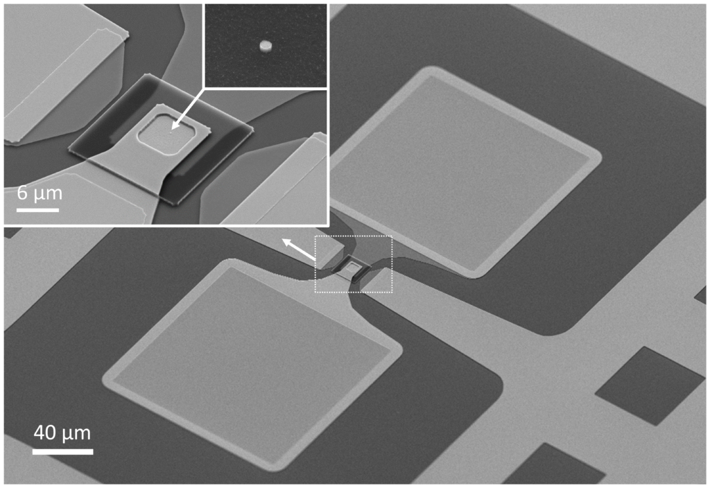
Scanning electron microscopy image of a MTJ device based on ITO top electrode process with FeCoB/MgO/FeCoB/[Tb/Co] magnetic stack with zooms on MTJ areas and the pillar prior the realization of the top electrode.
MRAMs have been moving up in the memory hierarchy in the last decades thanks to their non-volatility, low energy consumption, high endurance and its compatibility with silicon (Si) complementary metal-oxide semiconductor (CMOS) processing. To reach the processor and cache level, MRAM has to be written even faster, at pulse durations in the range of pico-and femto-seconds. This is the goal of the European FET project called SPICE, developing a spintronic-photonic IC platform to create world class ultra-fast and low power memory and sensor designs by combining spintronics (MRAMs) and photonics (crystal photonic) into hybrid circuits. To achieve this ambitious goal, we have developed an optical access to the spintronic element, i.e. a transparent and conductive electrode (TCO). In our work, we used a well-known material in the TCO family: the indium tin oxide (ITO) with the best transparency, low resistivity and easy to process.
By optimizing the ITO deposition conditions to obtain low resistivity (as low as 4.8×10⁻⁴ Ω.cm) and optical transparency (>80%), we have shown that it can be used as hard mask to pattern the MTJ pillars down to a diameter of 50 nm. We integrated it in the process and compared with our standard process based on tantalum (Ta) hard-mask, using a well-known reference magnetic stack based on [Pt/Co]/FeCoB/MgO/FeCoB MTJ. Electrical performances based on the tunnel magnetoresistance (TMR), key figure of merit in MRAM, are similar between the ITO and Ta based processes validating thus this new process flow.
A further step was achieved by integrating materials with optically switchable magnetization. These materials are multilayers of terbium and cobalt (Tb/Co) coupled with FeCoB free layer in a MTJ. By optimizing the materials and the ion beam etch (IBE) patterning, the new process flow was validated electrically achieving 28% TMR, demonstrating a process suitable and robust for different magnetic stacks. This work is novel, bringing closer the realization of faster MRAM based on spintronic-photonic hybrid circuits.
Team: MRAM, SPIN ORBITRONICS
Collaboration: Aarhus Universitet, IMEC, Radbout Universiteit, Quantum Wise
Funding: European Union’s Horizon 2020 research and innovation program under FET-Open
Grant Agreement No. 713481 (SPICE).
Further reading: Indium Tin Oxide (ITO) optical access for magnetic tunnel junctions in hybrid spintronic–photonic circuits, A. Olivier, L. Avilés Félix, A. Chavent, L. Álvaro-Gómez M.l Rubio Roy, S. Auffret, L. Vila, B. Dieny, R. C. Sousa and I. L. Prejbeanu, Nanotechnology (2020), DOI: 10.1088/1361-6528/ab9c56.
Contact: Ricardo Sousa