Topological insulators (TI) represent a new class of insulating materials hosting metallic surface states. Moreover, those surface states exhibit a Dirac cone energy dispersion where the strong spin-orbit coupling leads to a helical spin texture at the Fermi level. This property can be exploited to detect spin currents in conventional semiconductors like silicon or germanium. Here, we demonstrate the integration of the TI Bi2Se3 on a germanium platform and demonstrate the high spin current detection efficiency.
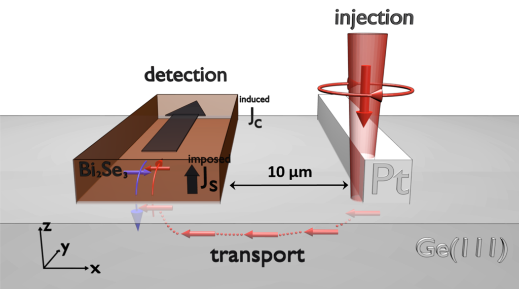
TIs hold great promises for new spin-related phenomena and applications thanks to the spin texture of their surface states. However, a versatile platform allowing for the exploitation of these assets is still lacking due to the difficult integration of these materials with the mainstream Si-based technology. Here, we exploit germanium as a substrate for the epitaxial growth of Bi2Se3, a prototypical TI. We probe the spin properties of the Bi2Se3/Ge pristine interface by investigating the spin-to-charge conversion taking place in the interface states by means of a nonlocal detection method. The spin population is generated by optical orientation in Ge, and diffuses towards the Bi2Se3 which acts as a spin detector (see figure). We compare the spin-to-charge conversion in Bi2Se3/Ge with the one taking place in Pt in the same experimental conditions. Notably, the sign of the spin-to-charge conversion given by the TI detector is reversed compared to the Pt one, while the efficiency is comparable. Due to the higher resistivity of Bi2Se3, the output voltage resulting from the spin-to-charge conversion is much higher than for platinum making Bi2Se3 an ideal spin detector on germanium. By exploiting first-principles calculations, we ascribe the sign reversal to the hybridization of the topological surface states of Bi2Se3 with the Ge bands. These results pave the way for the implementation of highly efficient spin detection in TI-based architectures compatible with semiconductor-based platforms.
Teams: 2D and semiconductor spintronics, Theory, Spin textures
Collaboration: Politecnico di Milano (Italy), PFNC
Funding: ANR TOP RISE
Further reading: Spin orbitronics at a topological insulator-semiconductor interface, T. Guillet, C. Zucchetti, A. Marchionni, A. Hallal, P. Biagioni, C. Vergnaud, A. Marty, H. Okuno, A. Masseboeuf, M. Finazzi, F. Ciccacci, M. Chshiev, F. Bottegoni, M. Jamet, Phys. Rev. B 101, 184406 (2020). DOI: 10.1103/PhysRevB.101.184406
Contact: matthieu.jamet@cea.fr, mair.chshiev@cea.fr
Figure: Sketch of the nonlocal spin injection detection scheme used in this work. The spin current is generated optically using optical spin orientation in Ge and Bi2Se3 plays the role of the spin current detector by inverse the Rashba-Edelstein effect.