
We have fabricated large-scale two-dimensional transition metal dichalcogenide (2D TMD) MoSe2, a promising candidate for electronics, valley-spintronics and optoelectronics, on insulating sapphire and have investigated its structural and transport properties. We have shown that the layered MoSe2 exhibits characteristics of a stoichiometric 2H-phase, a van der Waals epitaxy regarding the substrate and we have evidenced a hopping character for charge transport and an increase of conductivity of the layer under an application of magnetic field.
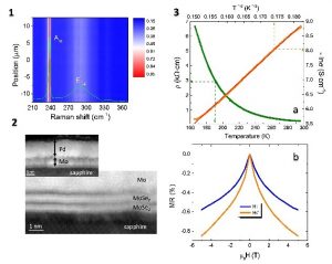
Figure 1 : Raman mapping of one monolayer MoSe2 along one direction x (y) showing microscopic homogeneity of the layer. Figure 2 : Cross sectional STEM image showing the van der Waals gap and interfaces between MoSe2, sapphire and metallic electrodes. Figure 3 : resistivity versus temperature with the fit (3a) and the negative MR measured at 250 K with in-plane and out-of-plane applied magnetic fields (3b).
The fast rise of semiconducting 2D TMD urges to look for artificial synthesis methods in order to achieve a large-scale and uniform 2D layers. So far, most of device demonstrations based on layered TMDs were obtained with exfoliated flakes which cannot be transferred to large-scale design and implementation into functional devices.
We have reported an alternative approach to fabricate MoSe2 layers down to one monolayer on sapphire substrates by using molecular beam epitaxy (MBE). Weak interactions between the substrate and the epilayer were expected, resulting in van der Waals epitaxy. The MBE technique allowed us to obtain millimetre-scale MoSe2 layers with a controllable thickness. The structural properties, identical to the bulk, the homogeneity of the layer were characterized using X-ray diffraction, Raman and photoemission (XPS) spectroscopies, scanning transmission electron microscopy (STEM). Contacting 2D layers with metallic electrodes remains a crucial challenge for the exploration of new physics in the TMDs. In our article, we have also addressed this issue by showing a good electrical contact between ultrathin layered MoSe2 and Pd/Mo stacks, which were successfully fabricated in-situ under UHV conditions. Thereby we have pointed out a variable hopping character of the charge carrier conductivity in the layered MoSe2. More interestingly, a magnetic field-dependent transport was investigated and a decrease in resistivity was observed for the first time in a MBE-TMD, stressing a fascinating feature of the charge transport in this system under the application of a magnetic field. The transport characteristics such as localization length, hopping length were considered for the discussion of the negative magnetoresistance. This negative magnetoresistance observed at millimeter-scale is similar to that observed recently at room temperature in WS2 flakes, highlighting the fact that the underlying physical mechanism is intrinsic to these two-dimensional materials and occurs at very short scale.
XPS measurements and STEM observations were carried out at the PFNC, CEA Grenoble.
Reference: M. T. Dau, C. Vergnaud, A. Marty, F. Rortais, C. Beigné, H. Boukari, E. Bellet-Amalric, V. Guigoz, O. Renault, C. Alvarez, H. Okuno, P. Pochet, and M. Jamet, Applied Physics Letters 110 , 011909 (2017)