
Magnetic spintronic memory called STT-MRAM have recently entered in volume production at major microelectronic foundries. The research in this area is now focused on preparing the future memory generations with higher capacity, higher speed, lower power consumption, wider range of operating temperature. To conduct this type of research, it is important to be able to accurately visualize the micromagnetic state of individual memory cell of dimensions down to 20nm. SPINTEC in collaboration with LETI and PFNC have demonstrated that this is possible by electron holography.
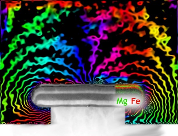
An off axis electron holography phase image of the magnetic stray field produced by the storage layer of a magnetic random access memory cell (STT-MRAM). The color-code depicts the orientation of the magnetic field lines and the grey-level image shows the MRAM device of 230 nm top-diameter together with its chemical analysis by Energy-dispersive X-ray spectroscopy (EDX).
Electron holography is shown to be an excellent tool for characterizing the micromagnetic state of the storage layer in magnetic memory cells by imaging the magnetic stray field surrounding the cell. The investigation has been conducted on MRAM cells realised by an innovative patterning approach which consists in depositing a magnetic stack on top of a T-shaped non-magnetic pillar. This nano-patterning approach avoids the difficult etching of the magnetic stack during processing and enables the realization of high density memory chips.
Electronic holography is an electron microscopy technique which allows to obtain information on the electric and magnetic fields seen by electrons as they pass through the sample. It is based on the interference between a beam passing through the sample and a reference beam. Team from SPINTEC and from LETI and the Nanocharacterization Platform (PFNC) have shown that this technique can be used to provide an image of the magnetic stray field around individual memory cells. The knowledge of this stray field allows, through modelling, to derive the micromagnetic state of the magnetic layers comprised in the memory cell, in particular of the storage layer. The study was performed on relatively large cells of diameter 230nm. However, from the obtained signal to noise ratio and thanks to contrast enhancement imaging technique, it was established that the technique could still be used for cells of diameters down to 20nm which are of industrial relevance for the development of MRAM of future generations. Besides, the influence of the memory temperature on the storage layer micromagnetic state could be investigated in-situ. It was observed that while in conventional MRAM, the storage layer magnetization points out-of-plane (up or down to represent logic “0” or “1”, above a certain temperature (in the range 150°C-250°C depending on sample composition), the storage layer magnetization tends to fall into the plane of the layers. This phenomenon is due to a thermal decrease of the perpendicular anisotropy existing at the interface between the magnetic storage layer and the tunnel barrier. This magnetization reorientation can lead to the formation of complex micromagnetic states (called C-state because the magnetization curls along the cell side as in a C-letter). These are valuable information which can be used to adjust the design of the memory cell. As a matter of fact, in MRAM cells, the storage layer magnetization has to remain out-of-plane and as uniform as possible.
Teams: MRAM, Spin textures, Spin orbitronics, Materials growth and Instrumentation.
Collaboration: CEA – LETI
Funding: ERC MAGICAL n°669204, ERC Holoview n°306535 and Carnot project MAGICMAPS
Further reading: An electron holography study of perpendicular magnetic tunnel junctions nanostructured by deposition on pre-patterned conducting pillars, V.Boureau et al, NANOSCALE, 12, 17312 (2020). DOI: https://doi.org/10.1039/D0NR03353G
Contacts: Bernard Dieny