
Creation of Magnetic Skyrmion Bubble Lattices by Ultrafast Laser in Ultrathin Films (December 18th, 2018)
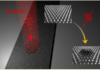
Magnetic skyrmions are topologically nontrivial magnetic domains where the magnetization rotates in a fixed sense (chirality). They are usually created by magnetic fields or by non-homogeneous electric currents. Here S.G. Je et al. have shown that hexagonal skyrmion bubble lattices can be locally generated with ultrafast (30 fs) laser pulses. Their original optical approach to […]
Read moreSingle-particle mass spectrometry with nanomechanical resonators (October 04th, 2018)
Mass spectrometry (MS) is an essential tool in a broad variety of fields, with good efficiency up to the kDa mass range (~10-21 g). We demonstrate here Nano-electro-mechanical systems mass spectroscopy (NEMS-MS) with arrays of individually addressed nanomechanical resonators, allowing for measurements in the MDa (~10−18 g) to GDa (~10−15 g) mass range. Monocrystalline silicon […]
Read moreHighly Efficient Spin-to-Charge Current Conversion in Strained HgTe Surface States Protected by a HgCdTe Layer (October 03rd, 2018)
We report the observation of spin-to-charge current conversion in strained mercury telluride at room temperature, using spin pumping experiments. We show that a HgCdTe barrier can be used to protect the HgTe from direct contact with the ferromagnet, leading to very high conversion rates. Conventional spintronics is based upon the use of magnetic materials to […]
Read moreSub-10nm thermally stable Perpendicular Shape Anisotropy magnetic memory (August 24th, 2018)
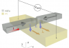
![]()
A new concept of thermally stable and electrically switchable Spin Transfer Torque Magnetic Random Access Memory (STT-MRAM) scalable to diameter down to 4nm was proposed and demonstrated. By dramatically increasing the thickness of the storage layer, a bulk magnetic anisotropy perpendicular to the plane of the layers can be induced which dramatically improves the memory […]
Read moreNonlinear properties of pure spin conductors (June 21st, 2018)
N. Thiery, A. Draveny, V. V. Naletov, L. Vila, J. P. Attané, C. Beigné, G. de Loubens, M. Viret, N. Beaulieu, J. Ben Youssef, V. E. Demidov, S. O. Demokritov, A. N. Slavin, V. S. Tiberkevich, A. Anane, P. Bortolotti, V. Cros, and O. Klein, Phys. Rev. B 97, 060409 (2018). N. Thiery, V. V. […]
Read moreDetection of Short-Waved Spin Waves in Individual Microscopic Spin-Wave Waveguides Using the Inverse Spin Hall Effect (June 21st, 2018)
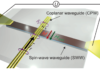
T. Brächer, M. Fabre, T. Meyer, T. Fischer, S. Auffret, O. Boulle, U. Ebels, P. Pirro, G. Gaudin, Nano Lett. 17, 7234 (2017) Detection of Short-Waved Spin Waves in Individual Microscopic Spin-Wave Waveguides Using the Inverse Spin Hall Effect We report on the wave-vector independent detection of short-waved spin waves with wavelengths down to 150 nm […]
Read moreSub-10nm thermally stable Perpendicular Shape Anisotropy STT-MRAM realized at SPINTEC (March 08th, 2018)
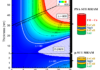
A team at SPINTEC in Grenoble has demonstrated thermally stable and electrically switchable Spin Transfer Torque MRAM (STT-MRAM) of diameter down to 4nm. Among the various technologies of non-volatile memories, STT-MRAM gathers a unique combination of assets: non-volatility, write speed (3-30ns), density (4Gbit demonstrated by Hynix/Toshiba), low consumption (a few tens of fJ/write), and very […]
Read moreGiant magnetoresistance in lateral metallic nanostructures for spintronic applications (January 22nd, 2018)
This study discuss the shift observed in spintronics from the current-perpendicular-to-plane geometry towards lateral geometries, illustrating the new opportunities offered by this configuration. The possibility to combine ultrathin magnetic and non-magnetic layers allowed creating hetero-structures whose dimensions are smaller than the characteristic lengths of the spin-dependent transport. This has notably led to the discovery of […]
Read moreEnhanced annealing stability and perpendicular magnetic anisotropy in perpendicular magnetic tunnel junctions using W layer (November 15th, 2017)
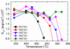
The stiffening of the perpendicular magnetic tunnel junction (pMTJ) stack resulting from the W insertion due to its very high melting temperature, is the key mechanism behind the extremely high thermal robustness. Thicker W layer in the W(t)/Ta 1 nm cap layer makes the storage electrode of pMTJ stack highly robust against annealing up to […]
Read moreElectrical detection of magnetic domain walls by inverse and direct spin Hall effect (August 28th, 2017)
Spin orbit torques allow to move efficiently DW in tracks made of ferromagnetic/spin Hall effect bilayer. Domain wall (DW) detection is then of great importance. In this letter, we demonstrate a detection method, based on the ability for a ferromagnetic nanowire, in which a DW is pinned, to inject or detect a pure spin current. […]
Read more