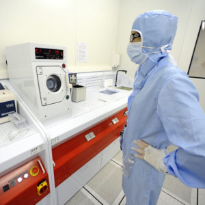
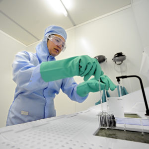
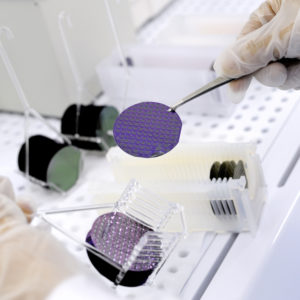
The PTA, Upstream Technological Platform, is a 1000 class clean room resulting from the pooling of technical and human resources of IRIG (Institut de recherche interdisciplinaire du CEA Grenoble) and LTM (Laboratoire des Technologies de la Microélectronique du CNRS, UJF et INP). The clean room extends over 700 m2, 350 m² on CEA site and 350 m² in the Grenoble INP site, within the CIME clean room ( InterUniversity MicroElectronics and nanotechnologies Centre).
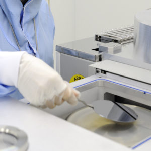
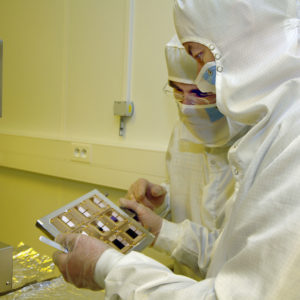
The PTA offers the technical capabilities needed to cover a wide range of projects in nanosciences andmicro- nanotechnologies: complementary methods and equipment facilities for lithography, deposition or etching enable reliable integration of nano-objects and nano-materials or patterning of thin layers in the nanometric range. The PTA can accommodate all types of substrates from small 5 x 5 mm² sample up to the 100 mm wafers. A huge diversity of materials can be processed within a reasonable approach of contamination management
The research fields are numerous: nanoelectronics, MEMS & NEMS, magnetism and spintronics, integration of nano-materials and nano-objects, photonics, … The purpose of the facility is both to provide the needed means and skills to researchers, and to welcome industrial companies looking for a place to develop theirprojects.
Flexibility, ease of access and use, are the cornerstone of the management of the PTA. This pooling of facilities between the major players of upstream research in Grenoble means that a specific management system had been set up combining INAC and LTM complementary views and needs: here, users will find both a state of the art facility and an optimal flexibility.

The Team


Recent news
- Spin-Hall Voltage over a Large Length Scale in Bulk Germanium (July 20th, 2017)
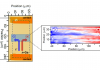
Germanium is one of the most appealing candidate for spintronic applications, thanks to its compatibility with the Si platform, the long electron spin lifetime and the optical properties matching the conventional telecommunication window. Electrical spin ... - Nanotweezers and their remote actuation by magnetic fields (May 23rd, 2017)
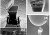
We have developed arrays of innovative magnetic nanotweezers or “nanojaws” on silicon wafers, by a top-down approach using the fabrication techniques of microelectronics. The mechanical manipulation of micro- and nanometric objects relies on constantly evolving techniques, ... - Magneto-optical micromechanical systems for magnetic field mapping (February 17th, 2017)
Magnetic field mapping techniques have continuously been developed due to the necessity for determining the spatial components of local magnetic fields in many industrial applications and fundamental research. Several factors are considered for sensors such ... - Misalign to write faster (October 17th, 2016)
The writing in conventional magnetic memories based on magnetic tunnel junctions (STT-MRAM) is intrinsically stochastic : a large amplitude thermal fluctuation is required to trigger the siwthing of the storage layer magnetization. SPINTEC has shown ... - Comparison of the use of NiFe and CoFe as electrodes for metallic lateral spin valves (May 17th, 2016)
A CoFe based ferromagnetic alloy has been used in lateral spin valves to replace NiFe alloys, which are overwhelmingly exploited as ferromagnets electrodes in lateral spintronic devices. By using this second material, emitted signals are ...